Now comes the fun part, at least for me. It’s time to design your PCB and start routing traces. This is where everything stops being abstract and turns into something real.
To get started, head up to the top bar and click Convert Schematic to PCB. That will open the PCB editor. You’ll see a pop up asking you to confirm the import of changes. Just hit Apply Changes, and you’re ready to begin laying things out.
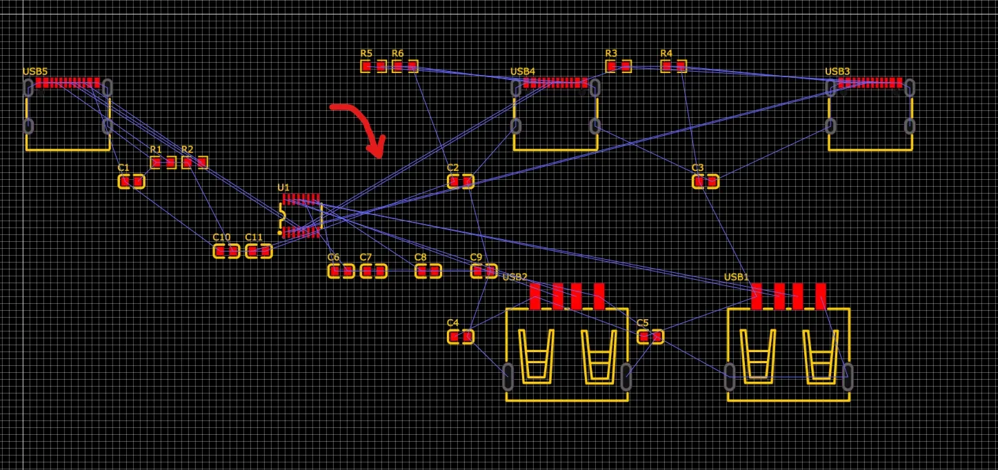
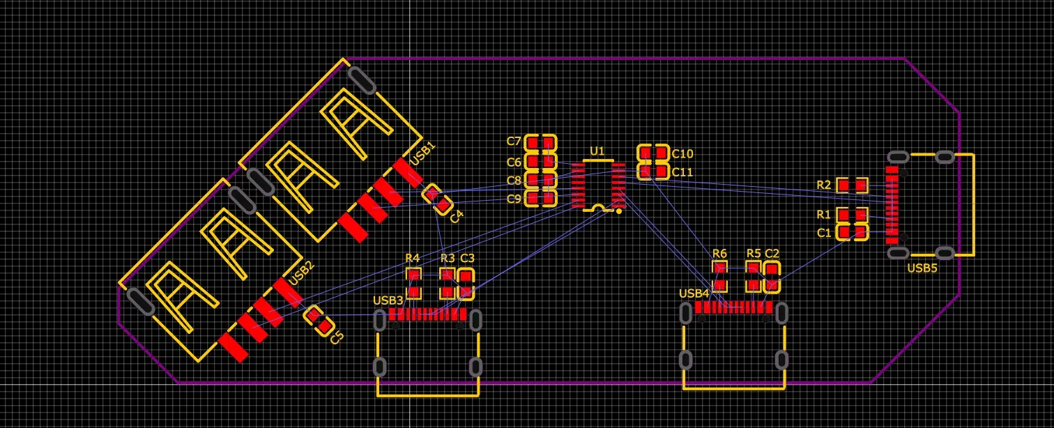
When the PCB editor opens, you’re going to be greeted by what looks like total chaos. Components scattered everywhere like they were dropped from the sky.
And then you’ll notice a bunch of thin blue lines crisscrossing the screen. Those are called ratlines. Think of them as little reminders saying, “Hey, this pad still needs to connect to that pad.” They don’t represent real copper yet. They’re just showing you the connections that exist in your schematic but haven’t been physically routed on the board.
Before you start dragging parts around, here’s a small tip that will make your life much easier.
At the beginning of a design, it’s usually best to hide the ground ratlines. Ground connects to a lot of things, so those lines tend to clutter the screen and make everything look more overwhelming than it actually is. Since ground is often handled cleanly at the end, hiding it for now helps you focus on the more critical signal connections first.
To do this, go to the left sidebar and open the Net tab. Expand the Ratlines section, find the GND net, and toggle its visibility off.
Planning it out
Now hold on. Before you start routing traces everywhere, you need to place your components properly.
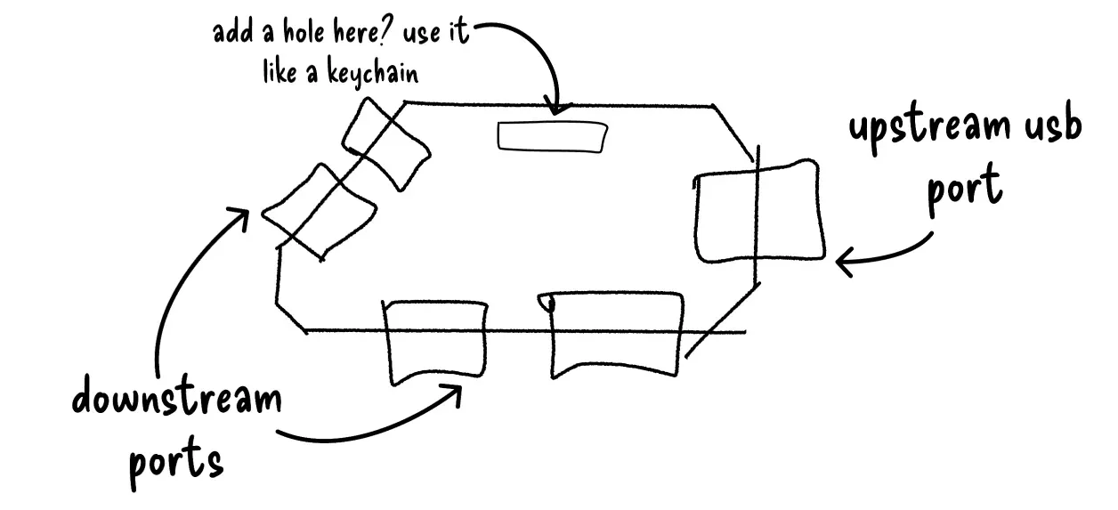
Good layout starts with intention. Take a moment and think about what you actually want this board to look like. Is it going to be a plain rectangle that quietly does its job? Sure, that works. But where’s the fun in that?
This is your project. Give it some personality. Maybe it’s a fun shape. Maybe it’s something you can turn into a keychain. Maybe it’s completely ridiculous in the best possible way. I’m turning mine into a small keychain shaped board, but you’re absolutely encouraged to design something wild.
If you want to go further and experiment with more advanced outlines, like silhouettes or detailed drawings, check out the little side guide on creating custom board shapes. You can get surprisingly creative with PCB outlines.
Personally, I’m aiming for something that looks a bit like this…
To make that happen, we need to define the shape of the board.
Select the Board Outline tool and choose the Polygon option. Alternatively, you can click directly on the Board Outline layer and use the Polyline tool to draw your shape manually.
From there, just start clicking to place points and sketch out your design. Think of it like connecting dots to carve out the silhouette of your board. Take your time and adjust the corners until the shape feels right. This outline is literally the boundary of your creation, so make it nice!
And don’t stress about getting it perfect on the first try.
The board outline isn’t fixed. You can always come back later and tweak it, adjust curves, move corners, or completely reshape it if inspiration strikes. Think of it as a flexible frame rather than a final decision.
Layout
Once your board outline is sketched out, it’s time to place components. This step matters more than anything else. Good placement is what separates a clean, professional board from a frustrating mess. When layout is done right, routing feels smooth and logical. When it’s done poorly, routing becomes a pain.
Be intentional. Think in functional groups. The way components are connected in the schematic should guide how they sit on the PCB.
Take the USB upstream connector as an example. In the schematic, it had a capacitor and two pull down resistors tied directly to it. That’s a small functional cluster. On the PCB, those passive parts should be placed close to the connector.
Here’s a helpful workflow: go back to the schematic editor and select the entire USB C upstream port circuitry as a group. Then switch over to the PCB editor. You’ll see that those corresponding components are now highlighted. This makes it much easier to grab them, move them together, and place them on your board.
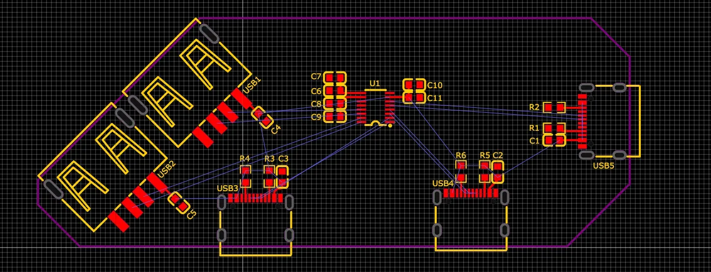
Now that my USB-C circuitry is selected, I’m going to drag it over to roughly where I want it on the board. Don’t worry about getting it perfect just yet, we’re just finding a good place for this little cluster before fine-tuning placement.
Next, I’ll position the USB-C connector so it sticks out slightly over the edge of the board. Then I’ll place the resistors and capacitor close to their respective pins.
Now I’ll tidy up the silkscreen designators, moving them so they’re nicely aligned and easy to read.
Here, you can use the Align tool to straighten things up and make everything look neat. Totally optional, but it gives your board a cleaner, more organized appearance.
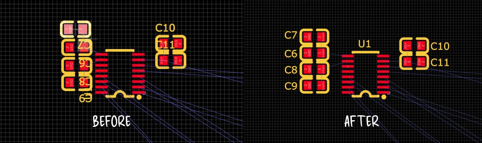
Next, I’ll place the USB hub IC along with its supporting circuitry inside the board outline.
Now I’ll rotate the IC to figure out which orientation makes connecting a wire from the USB upstream connector easiest. Turning it 90 degrees works perfectly, letting the USB data pins run straight from the IC to the connector.
Next, I’ll place the decoupling capacitors for the USB hub IC. Keep in mind that proximity matters. A capacitor that’s too far from the chip pin won’t do much. Try to keep each one as close to its pin as possible, but don’t put it directly on the pin. Leave a little space so it connects properly.
Once again, make sure nothing is overlapping. Take a moment to adjust the silkscreen designators, and space the capacitors just a little away from the IC so there’s room to route traces later.
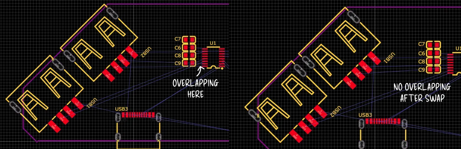
Now I’ll start placing the downstream ports. Be logical with their positions, keeping them where the ratlines stay mostly straight and don’t cross over other connectors’ ratlines.
Here’s an example. Right now my USB-A ports are laid out like this, and you can see the ratlines overlapping. If I swap the positions of these two connectors, the ratlines become much cleaner.
Notice how I’m running short on space and one of my USB connectors is hanging off the board. I can fix this by extending the board outline and making it a bit bigger. Like I mentioned earlier, the board outline isn’t fixed, and it’s normal to adjust it as the design progresses.
Now I’ll go back to the schematic and bring in the supporting pull down resistors and decoupling capacitors, placing them close to their respective connectors.
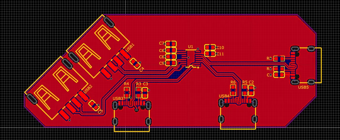
In the end, your board should look something like this. Every power pin should have a decoupling capacitor nearby, and the USB-C connectors should have the correct pull down or pull up resistors in place.
Routing
Now we move on to the fun and satisfying part: routing! To start, you can use the Routing tool on the top bar or just hit Alt + W.
I’ll start by connecting all the passive components to their USB connector for now. This gives me something like this. I’m not worrying about the data pins or connecting all the 5V traces just yet.
Now let’s focus on routing the data pins. USB data pins are routed as a differential pair, which is basically two wires, one positive and one negative, running side by side. This setup lets the signals travel faster and resist noise better.
To route them as a differential pair, go to Route → Differential Pair or just press Alt + D. Starting at the IC, I’ll select the DP pin. A pop-up will appear, and I’ll create the differential pair by selecting the DN pin as the negative net and then pressing Process.
Once routed, you’ll see two wires running side by side as a differential pair. I’ll then wire this straight over to the USB-C connector.
Now I’ll exit differential routing and switch back to single routing by selecting the Single Routing tool or pressing Alt + W. Then I’ll go to the USB connector and wire the DP and DN pads together as shown below.
Now I’ll repeat this step for the rest of the USB connectors, wiring their differential data pins in the same way.
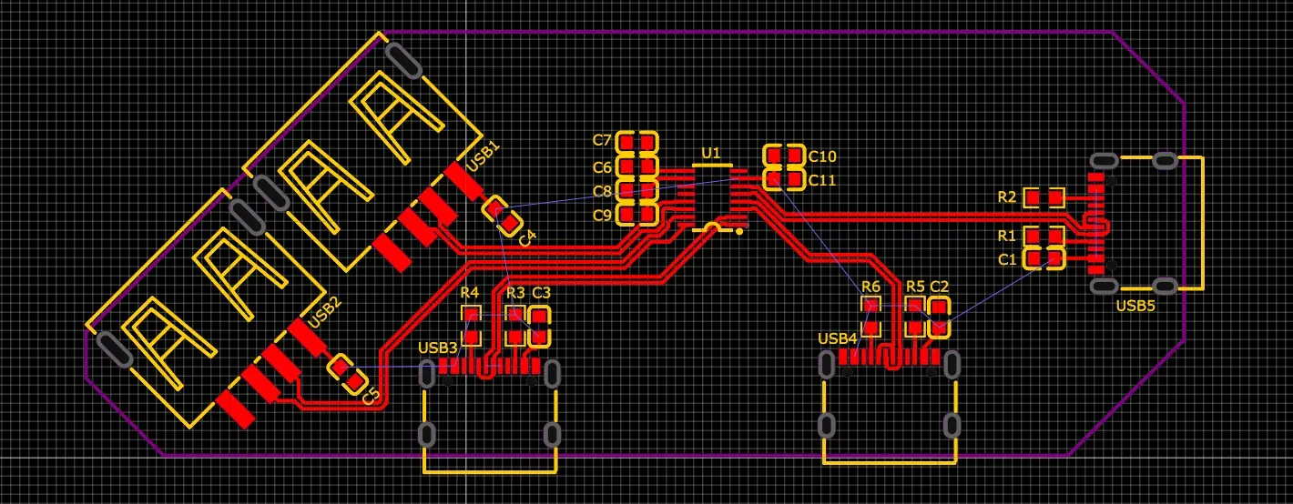
Now you might run into a situation with a USB-C connector where you can’t connect the data pins directly. Don’t worry. Our PCB has two layers, so we can switch to the back layer and then back up to the front layer to make the connection. This is done using a via, which you can place by pressing Alt + V while routing.
There we go, the connections are complete.
Next, I’ll route all the remaining differential pairs, and we end up with something like this.
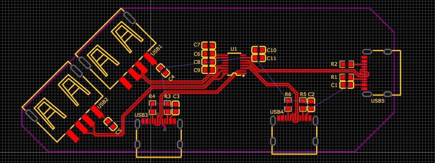
Now all that’s left is routing the 5V and ground lines. Before we start, let’s turn the GND ratlines back on.
Now for the 5V and ground connections, we’ll use a copper pour since there are lots of pads to connect. A copper pour basically fills an area of the board with copper for a specific net, which in this case will be 5V on the top layer and ground on the bottom layer.
We’ll start with the 5V pour on the top layer. Select the Copper Area tool from the top bar and draw a rectangle covering the board. When you left-click to confirm the shape, a dialog will appear. Make sure the layer is set to Top Layer and the net is +5V, then click Confirm. The tool will automatically fill the area with copper connected to the 5V net.
Now we’ll do the same for the bottom layer. Switch to the bottom layer using the layer side panel, then follow the same steps as before. This time, make sure the layer is set to Bottom Layer and the net is GND. The area will fill with copper connected to ground.
We’re not done yet. Most of our ground pads are on the top layer, and we only poured copper on the bottom, so they aren’t connected.
Go back to the top layer, route a trace from a ground pad, extend it a bit away from the pad, and press Alt + V to place a via connecting it down to the bottom layer.
Now just repeat this for all the ground pads on the top layer. Eventually, you’ll end up with something like this. Try to place one via per pad whenever possible, and avoid sharing the same via between multiple components.
For the USB-C connectors, you can simply connect the ground pads directly to the shield holes.
You’re almost done, but there’s one last step. Every time you add wires, vias, or make changes, you need to rebuild your copper zones to update them. Just press Shift + B to do this, and you’ll see the updated layout. This step is crucial, so don’t forget to rebuild zones after moving anything.
Now let’s jump into the 3D viewer and take a look at how our board is looking!
Looking pretty sick!
At this point, you’re basically done and could go ahead and order your board. But if you want to add some extra style, keep reading this guide.
Adding a keychain slot
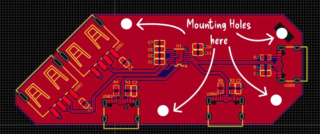
At the beginning when I was planning out layout, I sketched a small hole in the PCB so it could double as a keychain. Now it’s time to actually add that slot to the board. If you are not into the keychain idea, you can still add mounting holes, which I highly recommend. If you ever decide to design an enclosure later, mounting holes make it much easier to screw the board into a case and keep everything secure.
To add a slot, head to the top toolbar and choose the slot region tool. Draw a small rectangle where you want it, then tweak the position until it looks right.
After that, just fine tune the size and make sure it is not too close to the edge or any components.
Now if you open the 3D viewer again, you’ll see your updated PCB with the slot in place.
If you are not into the keychain idea but think you might design a case later, I strongly recommend adding mounting holes. The process is almost the same, except this time you choose a circle instead of a slot from the same tool menu.
When you place it, you will need to enter a radius. That value depends on the screw you plan to use, such as M2, M2.5, or M3. The M number refers to the screw’s diameter in millimeters, so an M2 screw has a 2 mm diameter. If you are using M2 screws for mounting, setting the radius to about 1.1 mm is a good choice.
At a minimum, I suggest adding at least two mounting holes, but if you have the space, four is even better. For placement, spread them out and choose strategic positions. In my case, these spots would make the most sense if I were adding mounting holes.
Silkscreen
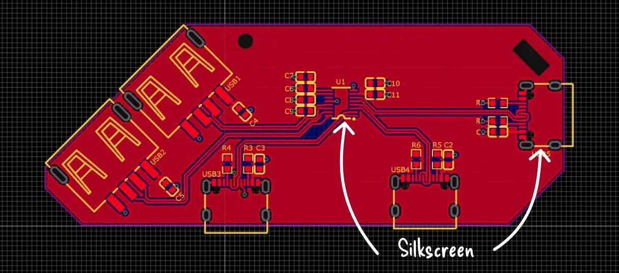
Now what is a PCB without some funky, cool silkscreen on it? As mentioned earlier, silkscreen is the layer printed on top of the solder mask. It is used for reference designators like C1 and C2, along with all the yellow markings you see on the board.
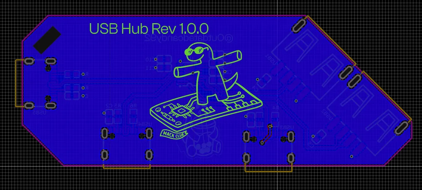
But you can also add your own text and illustrations to give it a little personality.
To do that, select the top silkscreen layer, choose the text tool, type in whatever you like, and place it on the board.
Custom text is fun, but adding your own graphics is even better. To do that, go to File → Import → Image and select the image you want to use. Remember that silkscreen is a single color, so it is best to choose an image that is already black and white. If you import something with lots of color, the EDA tool will convert it to black and white automatically, which can sometimes create strange artifacts.
I am going to place an image of Orpheus on the front. When inserting the image, start with a small size, around 20 mm wide or so. You can always resize it later, but starting smaller makes it easier to position and fine tune.
Make sure your silkscreen does not overlap with any other silkscreen in the area, and you should be good to go.
Open the 3D viewer to check out your new silkscreen design and see how it looks on the board.
If you peek in the 3D viewer, you’ll notice the back side is basically empty with no graphics. Let’s fix that. Go back into the PCB editor, select the bottom silkscreen layer, and add some designs to it.
You’ll notice that everything you add looks reversed. That’s because it’s the back side. To fix it, use the flip board tool on the top toolbar to turn the board around.
Now I’ll follow the same steps I used for the top layer and add some designs to the bottom. Once I’m done, I end up with something pretty cool like this.
Polishing
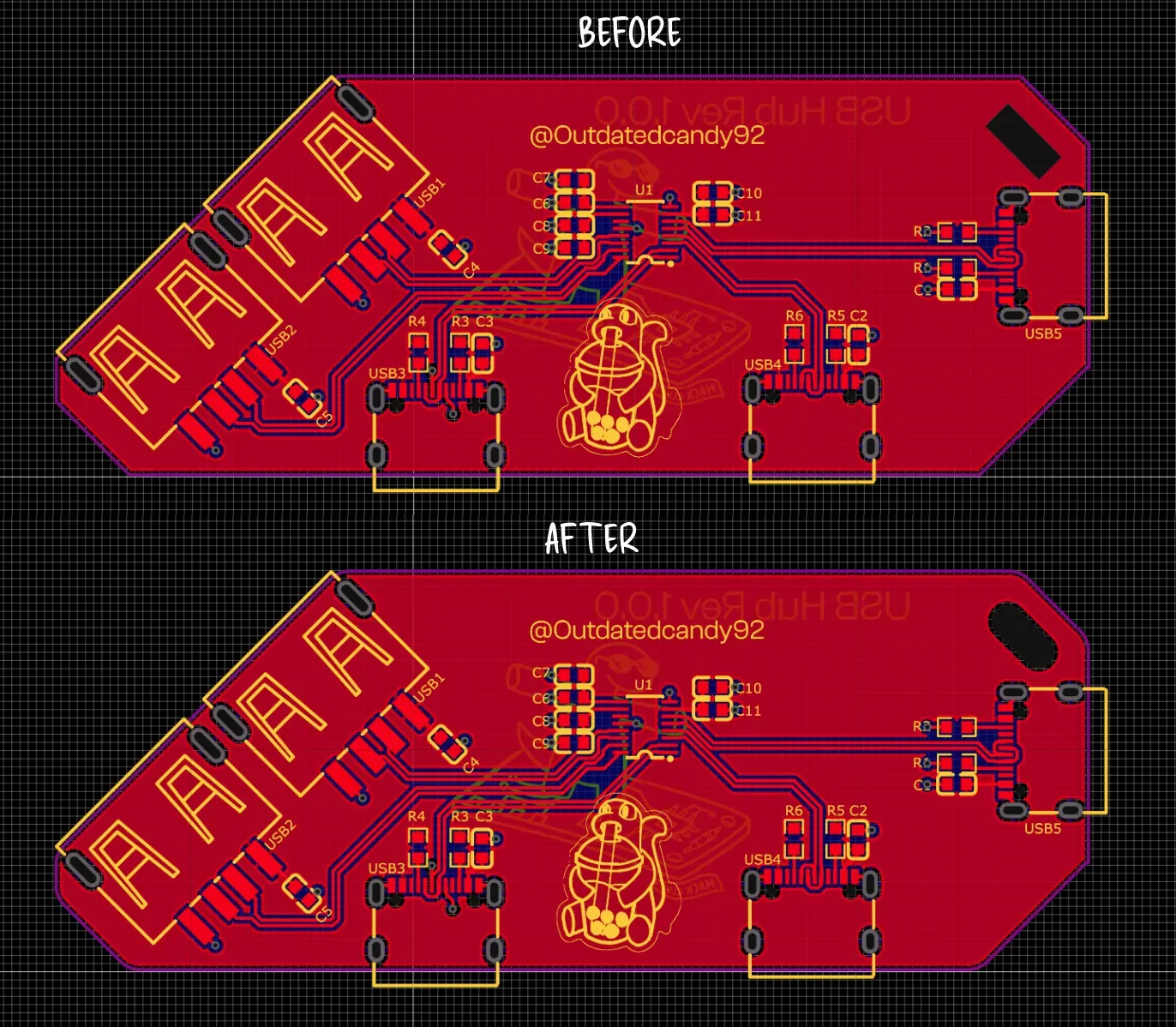
Before we order our boards, there are a few small touches you can add to make them look more polished, like filleting the edges.
Filleting rounds off the edges. By default, PCBs have sharp corners, which not only look harsh but can actually poke you.
To fillet your board outline, select it, right-click, choose Add → Fillet, and set the radius to whatever you like. I’m going with 2 mm.
I’ll also add some fillets to the slot on my board.
Remember to always rebuild your zones by pressing Shift+B.
Notice how much cleaner our board looks now!
At this point you’re done with your board! You can now go ahead and order it using JLC!