As we talked about earlier, the schematic is the blueprint for your PCB. It tells the board editor what connects to what, so if the schematic is messy or wrong, your PCB will be too. That’s why it’s important to keep it clear, tidy, and easy for someone else to understand at a glance.
Alright, let’s jump in. Open up the schematic editor and let’s get started.
Placing symbols
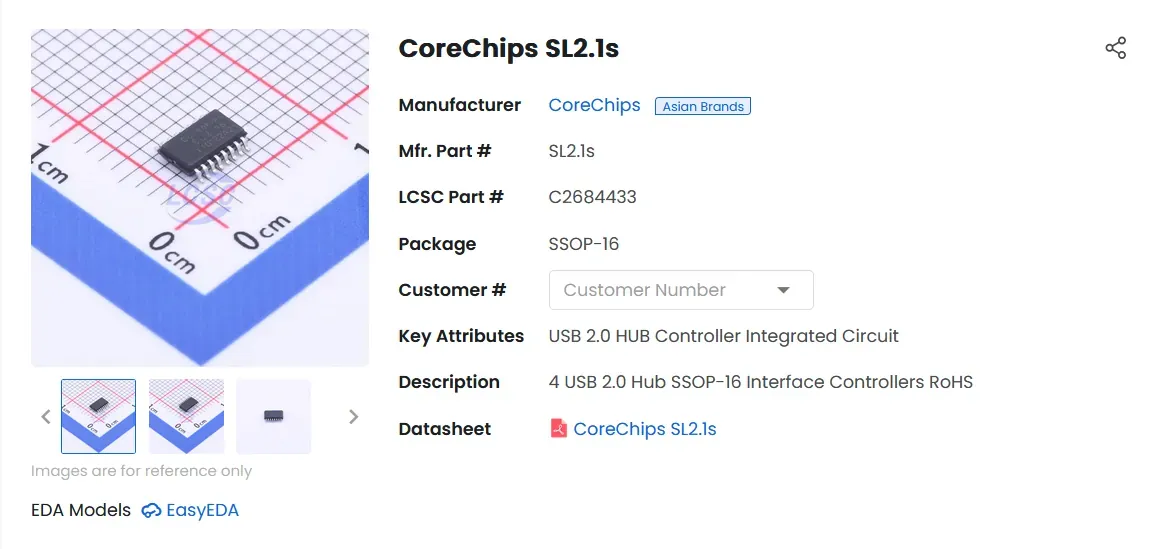
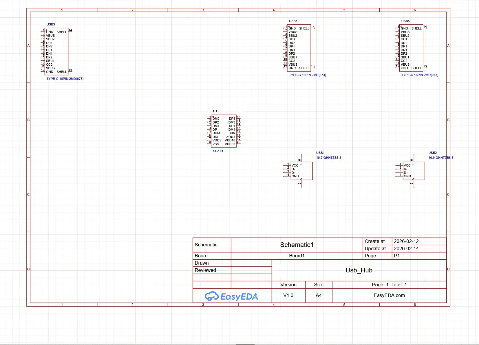
For this USB hub, we’re going to use the SL2.1S from CoreChips. This tiny chip is where all the magic happens. You plug one USB connection into it, and it splits that single port into four usable USB ports.
Since we’re having the board assembled by JLCPCB, the part number we’ll need is C2684433.
Let’s add the chip to our schematic.
Click the Component tool in the top toolbar, or just press Shift + F. In the search bar, type C2684433 and hit Enter. You should see the SL2.1S pop up in the results.
Click Place, move it onto your schematic, and left-click to drop it where you want. When you’re done, right-click to exit the placement tool. Just like that, the brain of your USB hub is now on the page.
Now that the main IC is on the schematic, let’s add the USB connectors, this is where you get to shape what your hub actually looks like.
The chip supports five total USB ports:
- 1 upstream port, which connects to your computer
- 4 downstream ports, where you plug in your devices
How you configure those ports is completely up to you. You could make everything USB Type C, everything USB Type A, or mix and match however you like. That’s part of the fun.
For my design, I’m using:
- 1 USB Type C for the upstream connection
- 2 USB Type C for downstream
- 2 USB Type A for downstream
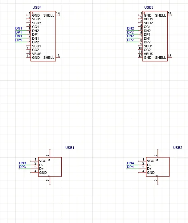
For the Type C connector, I’m using TYPE-C 16PIN 2MD(073) with part number C2765186.
For the Type A connector, I’m using 10.0 QHHTZB6.3 with part number C668591.
Go ahead and place your connectors based on the configuration you want. Once they’re on the schematic, you’ll clearly see the structure of your 1 in, 4 out USB hub coming together.
Schematics are typically read from left to right, kind of like a flow of information. Inputs on the left, processing in the middle, outputs on the right. Laying things out this way makes your design much easier to understand at a glance.
I’ll move my upstream USB Type C port to the top left, place the hub IC in the center, and arrange all the downstream ports along the right side. Now the data flow is visually clear: computer → hub chip → connected devices.
For parts like USB Type C and Type A connectors, the symbol already makes it obvious what they are. We don’t need huge manufacturer part numbers cluttering up the page and making the schematic harder to read.
To clean things up, hold Ctrl and select all of your USB connectors. Then, in the properties sidebar, untick the Manufacturer Part field. That hides the long part numbers from the schematic view without deleting any actual data.
The goal here is readability. A clean schematic is much easier to debug, share, and come back to later without giving yourself a headache.
There, its so much cleaner now!
Putting it together
Now that all the parts are on the page, it’s time to wire everything up.
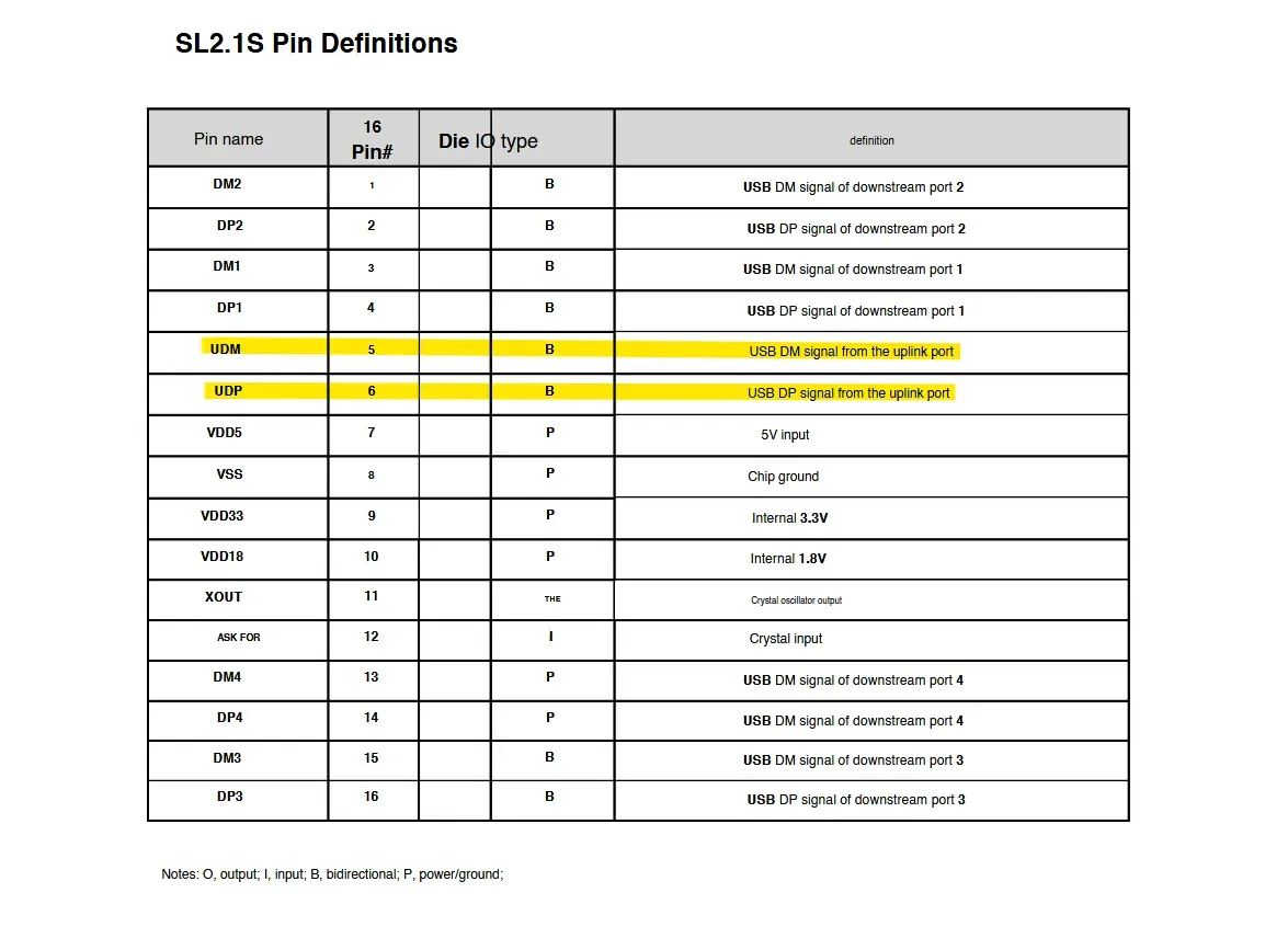
At this point you might be wondering how you’re supposed to know what connects to what. This is where datasheets become your best friend. Every manufacturer provides one, and inside you’ll find pin descriptions, example circuits, electrical specs, and usually even a reference design. The pin definitions section is what we care about right now. That’s your map.
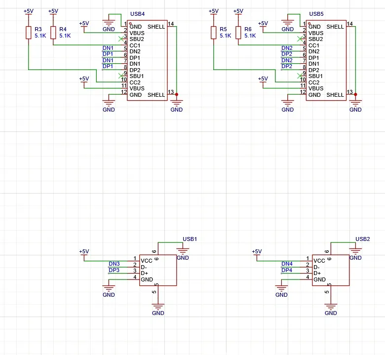
Let’s start with the upstream USB Type C port. If you search for USB C pin definitions, you’ll find plenty of diagrams explaining each signal in detail. When you look at the symbol in your schematic, you’ll notice something interesting: pins like DP1 and DP2, CC1 and CC2, and so on.
That duplication exists because USB Type C is reversible. The connector has matching pins on both sides so it works no matter which way you plug the cable in. Electrically, they serve the same purpose, but they’re duplicated to support flipping the connector.
Here’s a quick breakdown of the key USB Type C pins you’ll see on the schematic:
-
DPx / DNx – These are the data lines. They carry the actual information back and forth across the USB cable.
-
CC1 / CC2 – Channel Configuration pins. They handle things like negotiating power delivery and other USB-C features, but for our hub project, we won’t worry too much about those extras.
-
SBU1 / SBU2 – Sideband Use pins. These come into play for alternate modes like DisplayPort or can carry audio signals.
-
VBUS – This is the voltage supply, usually 5 V.
-
GND – Ground, your 0 V reference point.
-
SH – Shield. This is the metal casing around the connector that helps with grounding and protects against interference.
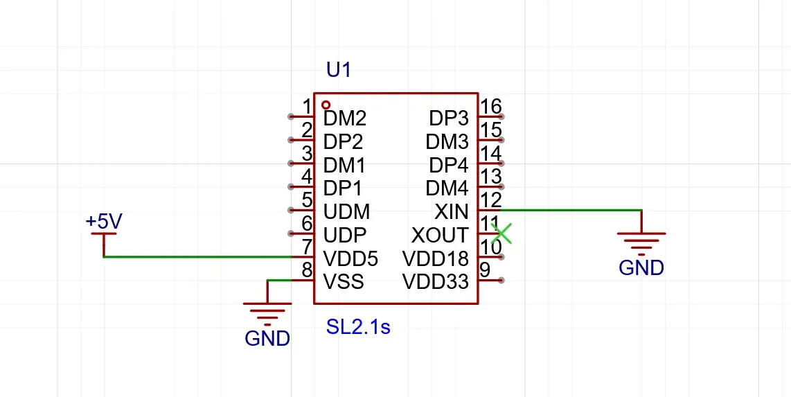
Let’s start wiring with power, since it’s a bit special. Because we use it so often, schematics have dedicated symbols for ground and power to keep things tidy.
Before we connect anything, I’ll rotate the USB-C symbol 180° by selecting it and pressing Space twice so the pins face the right way. This way, our wiring can flow neatly from left to right.
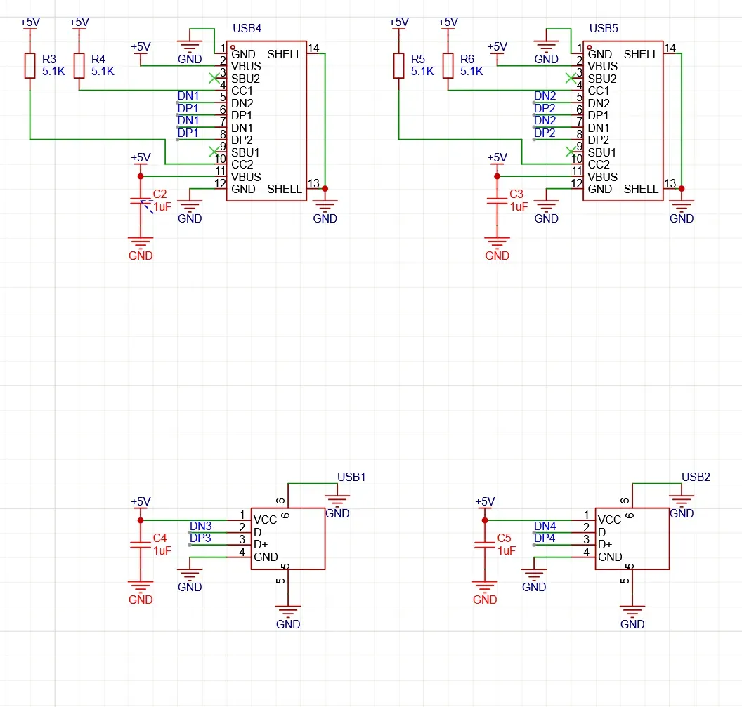
To start, we’ll tie all the VBUS pins together using a +5 V power flag. Click on the tool in the top toolbar labeled VCC, choose 5 V, and place it on the first VBUS pin. To keep the schematic clean, I like to move the flag slightly away from the pin so it’s readable. Repeat this step for all remaining VBUS pins on the connector.
Now all your VBUS pins are connected to +5 V, giving your hub a proper power supply to work with.
Next up is ground. Just like we did with VBUS, we’ll connect all the GND pins using ground flags.
Be careful to keep the wires and flags neat. Don’t let them overlap or cross unnecessarily. A messy tangle makes the schematic hard to read and can confuse anyone trying to follow your design later. Clean, spaced-out connections keep everything understandable and professional looking.
Now we’ll connect the SH (shield) pins to ground.
Select the Wire tool and draw lines from each SH pin to a GND flag. This grounds the metal shielding on the connector, which helps reduce interference and keeps your hub electrically stable.
Next up are the SBU1 and SBU2 pins. For our hub, we won’t be using them, but leaving pins completely floating is generally bad practice.
To handle this, we’ll use a No Connect (NC) flag. Select it from the top toolbar and place it on both SBU1 and SBU2 pins. This clearly signals that these pins are intentionally unconnected, keeping your schematic clean and professional.
Now let’s handle the CC1 and CC2 pins. These pins basically tell the host “hey, I’m a downstream port and I need some current.” To do this, we use 5.1 kΩ resistors connected to ground, these are called pull-down resistors because they “pull” the voltage down to 0 V.
Here’s how to add them:
-
Select the Resistor tool from the top toolbar.
-
Place two resistors pointing down, that’s the standard way to show a pull-down in schematics.
-
Select each resistor and change its value to 5.1 kΩ.
-
Wire one end of each resistor to a CC pin and the other end to a GND flag.
And just like that, your hub politely asks for power whenever a device is plugged in.
Now it’s time to handle the data pins. These need to connect to the SL2.1S chip, but since the IC is a bit far away on the schematic, we don’t want a spaghetti mess of wires. This is where net labels come in, they let you connect signals “virtually.” Any pins with the same net label are electrically connected, no matter where they are on the schematic.
Here’s what we’ll do:
-
Place a net label on DP2 and double-click it to rename it DP (for Data Positive).
-
Copy that label and paste it onto DP1.
-
Do the same for DN1 and DN2, renaming the label DN (for Data Negative).
Make sure the labeling is correct: DP goes on both DP1 and DP2, and DN goes on both DN1 and DN2. Once that’s done, these signals can be “connected” to the hub IC cleanly, without any messy wires crossing the schematic.
Next, let’s tackle the SL2.1S itself. To figure out how to wire it up, the datasheet is your best friend, it tells you exactly what each pin does and how it should connect.
A quick way to get there is to click on the IC symbol, then in the Properties tab click on the device link. This will take you to its LCSC page, where you can find and open the official datasheet. Once you have it open, you’ll be able to see all the pin assignments and recommended connections for your USB hub.
The original datasheet is partly in Chinese and partly in English, so if you can’t read it, a quick trick is to download the PDF and use Google Translate to get a full English version. For convenience, here’s a translated version you can use: [link].
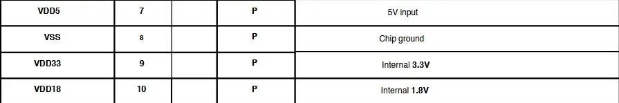
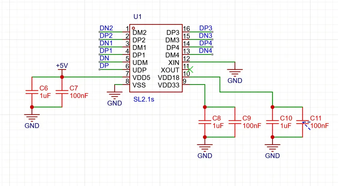
Scroll down to the pin definition table, this is the map we’ll use to figure out all the connections. Starting with power:
-
VSS – Ground (GND)
-
VDD5 – 5 V input for the chip
-
VDD33 – 3.3 V internal supply
-
VDD18 – 1.8 V internal supply
These pins make sure the IC gets the right voltages it needs to run.
Let’s connect the power pins on the IC:
-
Tie VSS to GND.
-
Connect VDD5 to the +5 V power flag.
The VDD33 (3.3 V) and VDD18 (1.8 V) pins are generated internally by the IC, so for now we can leave them unconnected. They’ll take care of themselves once the chip powers up.
Next, let’s look at the XOUT and XIN pins, they’re for connecting an external crystal.
Every chip needs precise timing to communicate and operate correctly, and that timing comes from a clock signal. An internal clock is usually good enough for simple tasks, but it can drift and cause errors. That’s where an external crystal comes in, it’s like a super-accurate metronome, giving the IC a stable, exact frequency so everything stays perfectly in sync. Without it, the chip could run a bit too fast or too slow, which would break USB communication.
If we scroll down in the datasheet, it specifies a 12 MHz crystal oscillator. That means we need a crystal with a resonant frequency of 12 MHz to hook up to XIN and XOUT.
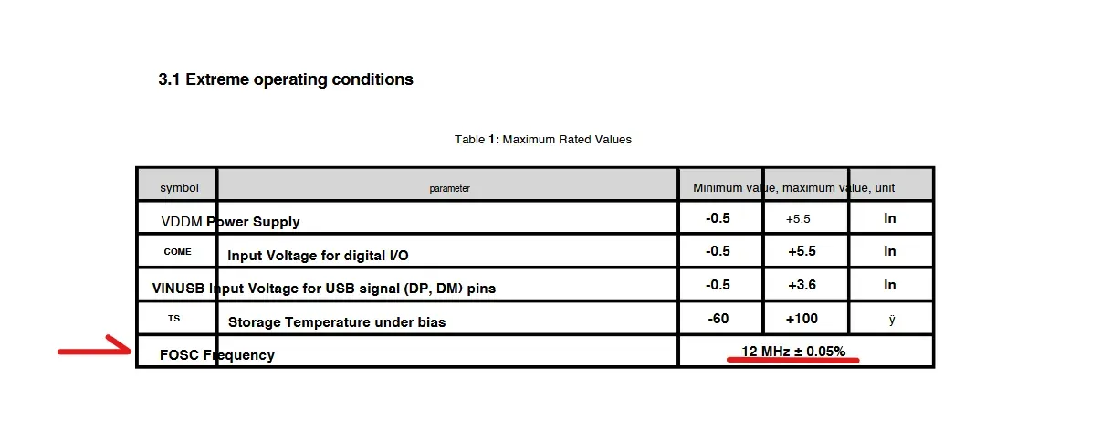
Normally, you’d add a crystal here, but this particular chip is known to work perfectly fine using its internal clock. That means we can skip adding the external crystal and let the IC handle timing on its own.
To keep the schematic clean:
-
Tie XIN to GND.
-
Place a No Connect (NC) flag on XOUT.
This clearly shows that the crystal isn’t used, while keeping your schematic neat and correct.
Looking back at the pin definition table, you’ll notice UDM and UDP, these are the USB D– and D+ signals from the upstream port, the one that connects to the host computer.
In other words, these pins are how your hub talks to the computer. Everything coming from or going to the host passes through UDM and UDP, so these are the signals we’ll connect to our net labels from the upstream USB-C port.
Now it’s time to hook up the data lines from our upstream USB-C connector.
You’ll notice a small naming difference: the connector has DP and DN, while the IC uses DP and DM. Don’t worry! DN and DM are the same thing; they both refer to the negative data line, while DP is the positive data line.
To connect them, simply copy the DP and DN net labels you placed on the USB-C connector earlier and paste them onto the corresponding DP and DM pins on the IC. This way, the upstream port is properly wired without any messy wires running across the schematic.
Finally, let’s connect the downstream data ports.
For each of the DPx/DMx pins on the IC, create net labels just like we did for the upstream port.
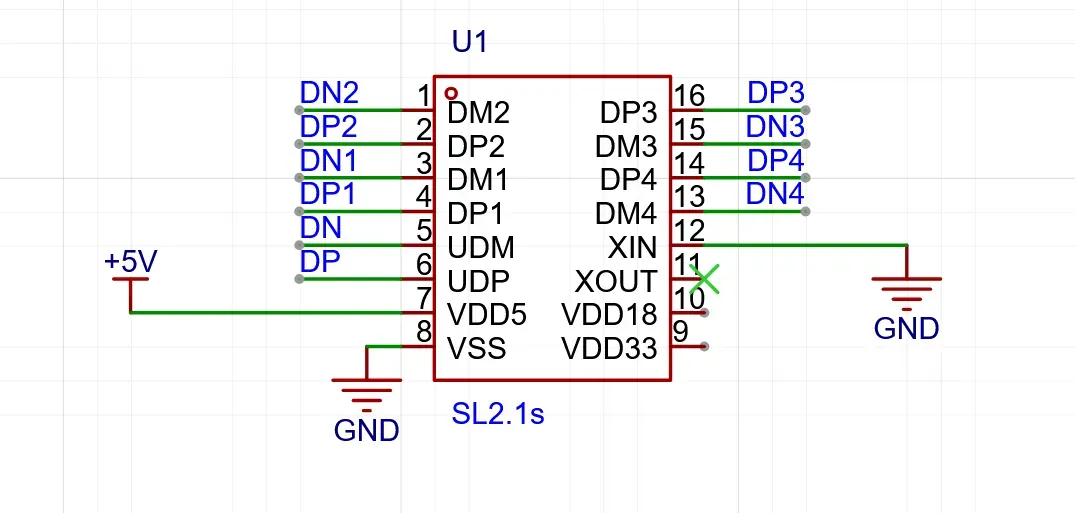
Once that’s done, connect each net label to the data pins of one of your four downstream USB connectors. Remember: each data pair goes to only one USB port! don’t share a pair between multiple connectors.
Next, finish wiring the remaining pins on your downstream USB connectors.
-
VBUS / VCC connects to +5 V.
-
GND and SH (shield) connect to GND.
-
For USB-C downstream ports, wire them the same way as the upstream port, except you’ll need to add 5.1 kΩ pull-up resistors on the CC pins instead of pull-downs.
For the USB-C downstream ports, the CC pins use pull-up resistors instead of pull-downs. The standard way to show a pull-up in a schematic is to have the resistor pointing up toward the voltage supply.
So for each downstream USB-C port, place a 5.1 kΩ resistor on the CC1 and CC2 pins, orient it pointing up, and wire the other end to +5 V.
If you’ve followed all these steps, your schematic should now look clean and complete, with all power, data, and control signals properly connected.
We’re almost done! The last little piece to add is capacitors, specifically decoupling capacitors.
Capacitors do two main things: they store energy and they let high-frequency signals pass through. We use these properties to our advantage by placing them on power rails, they help smooth out tiny voltage dips and filter out electrical noise, keeping our USB hub stable.
For this project, place 1 µF capacitors between VBUS (or VCC) and GND on each USB connector. This ensures each port gets clean, steady power and keeps the hub running reliably.
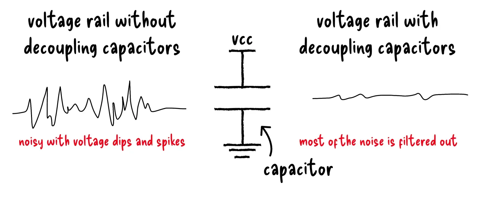
Basically, each decoupling capacitor will have one end connected to the power pin and the other end connected to ground.
A little schematic etiquette tip: power flags should point up and ground flags should point down. To keep things tidy, place your decoupling capacitors following this convention, power end toward the +5 V flag and ground end toward the GND flag. This makes the schematic easier to read and visually consistent.
For the IC’s internal supply pins, VDD33 (3.3 V) and VDD18 (1.8 V), we’ll add two capacitors each: a 1 µF and a 100 nF. Both act as decoupling capacitors, but the smaller 100 nF capacitor reacts faster to sudden voltage spikes, making it great for filtering high-frequency noise.
We’ll do the same thing for the VDD5 pin: a 1 µF and a 100 nF capacitor to ground. This keeps all the IC’s power rails clean and stable, ensuring reliable operation of the hub.
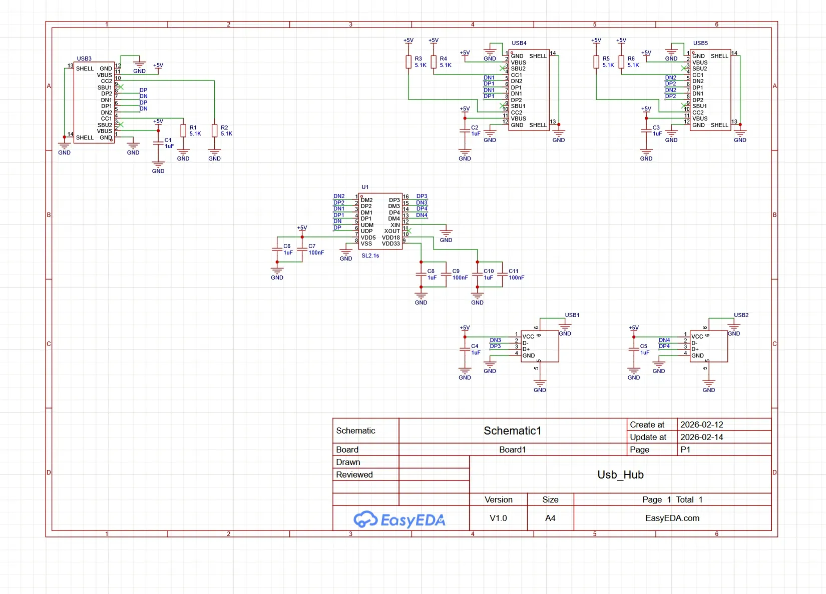
Here’s roughly what your completed schematic should look like at the end: all power rails, ground connections, data lines, pull-up/pull-down resistors, and decoupling capacitors in place, with clean left-to-right flow from the upstream port through the IC to the downstream ports. Everything should be neatly labeled and easy to read, ready for the PCB stage.
And just like that, schematics complete! :D
Don’t forget to save your work by pressing Ctrl + S so all your hard work is safe. Your USB hub is now fully laid out on paper, ready for the next step: designing the PCB.